
#Industry News
Gas Treatment Technologies for Cleanrooms and Semiconductor Fabs
Gas Treatment Technologies for Cleanrooms and Semiconductor Fabs
Modern semiconductor manufacturing depends on highly controlled gas delivery, purification, abatement, and monitoring systems to maintain cleanroom integrity and process yield.
The semiconductor industry operates at the frontier of precision manufacturing, where nanometer-scale device structures demand exceptionally clean environments and tightly controlled process conditions. In modern cleanrooms and wafer fabrication facilities, gases are indispensable for deposition, etching, cleaning, doping, and environmental control. However, these gases can also introduce contaminants, create safety hazards, and generate harmful exhaust streams. Consequently, gas treatment technologies have become a critical component of semiconductor infrastructure.
This article examines the technical principles, system architecture, and emerging trends in gas treatment technologies for cleanrooms and semiconductor fabs. It focuses on gas purification, distribution, exhaust treatment, monitoring, and safety systems that support advanced semiconductor manufacturing.
The Role of Gases in Semiconductor Manufacturing
Semiconductor processes rely on a wide variety of specialty gases. Common examples include:
Deposition gases
Silane (SiH₄), ammonia (NH₃), tungsten hexafluoride (WF₆).
Etching gases
Chlorine (Cl₂), hydrogen bromide (HBr), sulfur hexafluoride (SF₆), fluorocarbons.
Inert carrier gases
Nitrogen (N₂), argon (Ar), helium (He).
Cleaning gases
Hydrogen fluoride (HF), ozone (O₃), and related chemistries.
The purity requirements for these gases are extreme. Contaminants at parts-per-billion (ppb) or even parts-per-trillion (ppt) levels can cause wafer defects, reduce yield, and impact device reliability. Therefore, gas treatment systems must simultaneously address purity, safety, environmental compliance, and process stability.
Gas Purification Systems
Ultra-High Purity Requirements
Cleanroom gas purification begins with bulk gas supply and continues through the distribution network to the point of use. Semiconductor manufacturers typically require gases with impurity levels below 1 ppb for moisture, oxygen, hydrocarbons, and particles.
To achieve these specifications, fabs employ multiple purification stages.
Purification Technologies
Getter Purifiers
Reactive metal materials chemically bind impurities such as oxygen, moisture, and carbon compounds. Getters are widely used for nitrogen, argon, and hydrogen purification.
Adsorption Purifiers
Molecular sieves, activated alumina, and other porous materials remove water vapor and trace contaminants through physical adsorption.
Catalytic Purifiers
Catalysts promote reactions that convert impurities into removable compounds. For example, oxygen can be converted to water and subsequently removed by adsorption.
Particle Filters
Submicron and ultrafine filters capture particulate contamination generated during gas handling and distribution.
A typical gas purification train may combine several of these technologies to achieve the required purity level.
Gas Distribution in Cleanrooms
Material Selection
Gas distribution systems for semiconductor facilities are constructed using materials that minimize contamination and corrosion. Electropolished stainless steel (commonly 316L) is widely used because it offers:
Low surface roughness
Excellent corrosion resistance
Reduced particle generation
Compatibility with high-purity gases
Surface Preparation and Orbital Welding
Internal surface finish is critical. Electropolishing reduces microscopic defects where contaminants could accumulate. Orbital welding is preferred for joining tubing because it produces highly consistent, contamination-free welds.
Pressure Regulation and Flow Control
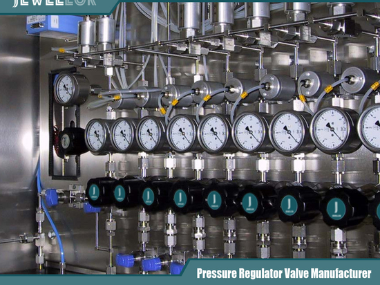
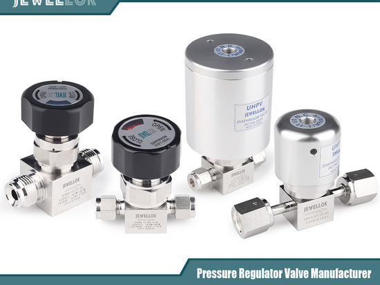
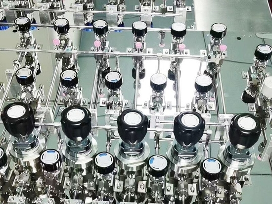
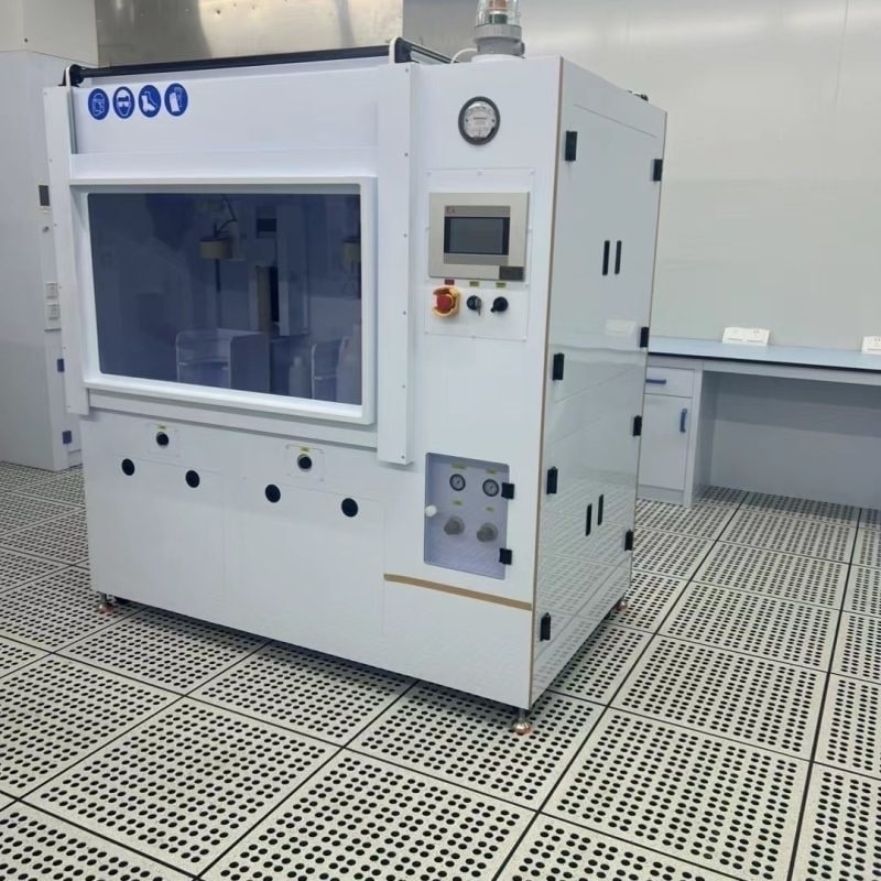
Semiconductor tools require stable gas delivery at precisely controlled pressures and flow rates. Gas cabinets, valve manifold boxes, and mass flow controllers (MFCs) are integrated into the distribution network to provide accurate process control while maintaining containment and safety.
Exhaust Gas Abatement Technologies
Process gases that exit semiconductor tools often contain toxic, corrosive, pyrophoric, or greenhouse gas components. Direct release to the atmosphere is unacceptable. Exhaust gas treatment systems, commonly called abatement systems or scrubbers, are therefore essential.
Wet Scrubbers
Wet scrubbers are commonly used to neutralize acid gases and soluble contaminants in semiconductor exhaust streams.
Wet scrubbers use liquid absorbents to remove soluble gases and particulates. They are effective for treating acid gases such as HF, HCl, and SO₂. The process typically involves:
Contacting the exhaust gas with a scrubbing liquid.
Absorbing or neutralizing contaminants.
Separating droplets from the cleaned gas stream.
Treating or recycling the spent scrubbing solution.
Wet scrubbers offer high removal efficiency but require water treatment infrastructure and careful management of secondary waste streams.
Dry Scrubbers
Dry scrubbers use solid sorbent materials to capture contaminants. They are commonly employed for lower flow rates and applications where liquid waste minimization is important. Sorbent cartridges must be periodically replaced when exhausted.
Thermal Oxidation
Thermal oxidizers destroy combustible and hazardous gases by high-temperature oxidation. They are frequently used for pyrophoric gases such as silane and hydrogen-containing mixtures. The oxidized products are then further treated to remove particulates and acid gases.
Plasma Abatement
Plasma abatement systems use energetic plasma to dissociate stable molecules, including perfluorinated compounds (PFCs). This approach is increasingly important because many fluorinated gases used in semiconductor etching have extremely high global warming potentials.
Treatment of Greenhouse Gas Emissions
Semiconductor manufacturing is a significant source of fluorinated greenhouse gases, including CF₄, C₂F₆, and NF₃. These compounds are chemically stable and difficult to destroy.
Modern fabs employ specialized abatement systems that combine plasma, combustion, and scrubbing technologies to achieve high destruction and removal efficiency (DRE). Regulatory pressure and corporate sustainability goals are driving continued investment in advanced greenhouse gas treatment solutions.
Gas Detection and Monitoring
Continuous monitoring is essential for both process quality and personnel safety.
Contamination Monitoring
Trace impurity analyzers measure moisture, oxygen, hydrocarbons, and particles in ultra-high-purity gas streams. Online monitoring enables rapid detection of contamination events before they affect production.
Safety Monitoring
Toxic gas detectors, combustible gas sensors, and oxygen deficiency monitors are installed throughout gas storage and distribution areas. These systems are typically integrated with facility safety controls to trigger alarms, ventilation, and automatic shutdown procedures.
Data Integration
Modern semiconductor facilities increasingly use centralized monitoring platforms that collect real-time data from gas analyzers, scrubbers, and process tools. Advanced analytics can identify trends, predict maintenance needs, and optimize system performance.
Cleanroom Air Management
While process gas treatment is critical, cleanroom air quality must also be maintained.
HEPA and ULPA Filtration
High-efficiency particulate air (HEPA) and ultra-low penetration air (ULPA) filters remove airborne particles from recirculated cleanroom air. Semiconductor cleanrooms often operate at ISO Class 3 or better, requiring extremely low particle concentrations.
Chemical Filtration
Molecular contaminants can be just as damaging as particles. Chemical filtration systems remove airborne acids, bases, and organic compounds that could affect sensitive processes such as photolithography.
Airflow Control
Laminar airflow, pressure differentials, and carefully designed ventilation systems help prevent cross-contamination between process areas and maintain cleanroom classification.
Safety Considerations
Gas treatment systems in semiconductor facilities must address multiple safety hazards:
Pyrophoric gases
Silane and similar gases can ignite spontaneously in air.
Toxic gases
Arsine, phosphine, chlorine, and hydrogen fluoride pose serious health risks.
Corrosive gases
Many process gases can damage equipment and infrastructure if not properly contained.
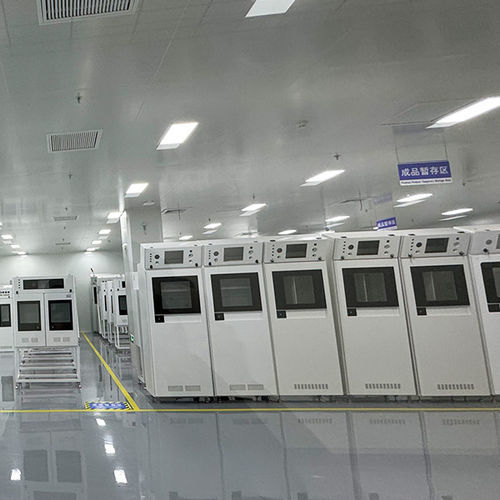
Engineering controls include gas cabinets with automatic shutoff valves, exhausted enclosures, leak detection systems, emergency ventilation, and redundant safety interlocks. Personnel training and strict operating procedures are equally important.
Emerging Trends
Digitalization and Predictive Maintenance
Industrial IoT technologies are being applied to gas treatment systems. Sensors continuously monitor flow, pressure, temperature, and contaminant levels. Machine learning algorithms can predict filter saturation, scrubber maintenance requirements, and potential system failures before they occur.
Energy and Resource Efficiency
Semiconductor fabs consume large amounts of energy, water, and specialty chemicals. New gas treatment technologies aim to reduce operating costs and environmental impact through:
Lower-pressure-drop filtration systems
Regenerable adsorbents
Water recycling in wet scrubbers
Heat recovery from thermal abatement units
Advanced Materials
Research continues into new sorbents, catalysts, and corrosion-resistant materials that can improve removal efficiency and extend equipment lifetime in harsh semiconductor environments.
Stainless Steel High Purity Two Stage Specialty Regulator
Stainless Steel High Purity Two Stage Specialty Regulator
Conclusion
Gas treatment technology is a foundational element of modern cleanroom and semiconductor fabrication infrastructure. The combination of ultra-high-purity gas delivery, sophisticated distribution systems, advanced exhaust abatement, comprehensive monitoring, and rigorous safety controls enables the production of increasingly complex semiconductor devices.
As process geometries continue to shrink and environmental regulations become more stringent, the demands placed on gas treatment systems will only increase. Future developments will likely focus on higher purity standards, improved greenhouse gas reduction, greater automation, and enhanced resource efficiency. For semiconductor manufacturers, investment in advanced gas treatment technology is not merely a compliance requirement—it is a strategic necessity for achieving high yield, operational reliability, and sustainable growth.
For more about gas treatment technologies for cleanrooms and semiconductor fabs, you can pay a visit to Jewellok at https://www.specialtygasregulator.com/product-category/specialty-gas-cabinet/ for more info.