#Product Trends
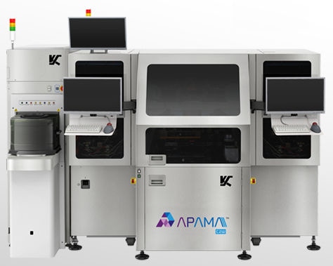
NEW: wafer substrate aligner / bonder by Kulicke & Soffa
MORE THAN BONDING
As features and functionalities of ICs increases, driving higher I/Os, the trend for flip chip is moving towards pitches less than 100 μm needing higher accuracy flip chip bonding and alternative interconnect solutions. Designed with performance and accuracy in mind, K&S APAMATM solutions provide higher accuracy and lower pitch bonding with market leading throughput.
The APAMA Series offers fully Automated Chip-to-Substrate (C2S) and Chip-to-Wafer (C2W) solutions for Thermo-Compression Bonding (TCB), High Density Fan-Out Wafer Level Packaging (HD FOWLP) and High Accuracy Flip Chip (HA FC).
COST-OF-OWNERSHIP ADVANTAGE
Modular designs allow the flexibility of upgrading from HD FOWLP or HA FC to TCB processes enabling effective cost-of-ownership and preserving the investments of our customers.

