#Product Trends
Push-Pull Capacitance Sensor Measures Un-grounded Targets
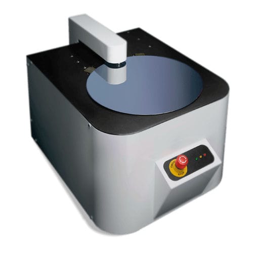
How to measure the thickness and warp of 156 mm² photovoltaic (PV) wafers with the accuracy of <1um, as they pass at the rate of one wafer per second ?
Today’s semiconductor and solar industries drive the demand for thinner wafers to conserve silicon and fulfill new IC applications. To meet this demand, wafer fabricators seek greater dimensional control of their silicon products. With that said, semiconductor wafers used to make integrated circuits (ICs) and silicon photovoltaic (PV) cells are fragile and expensive. The ability to precisely measure critical wafer parameters such as bow and warp not only ensures the integrity of circuit patterns, it improves yields and lowers production costs.
Non-contacting capacitance sensors offer the precision, accuracy, and speed needed to measure flatness, thickness variation, and other critical dimensions. Typically, the standard capacitance sensor acts as one plate of a classical two-plate capacitive gap measurement scenario. The grounded target – i.e. the silicon wafer – forms the second plate.
Grounding, however, presents challenges. First, it can scratch or damage the wafer which is fragile and expensive. Second, it prohibits those sensing scenarios where the wafer must be moved to acquire all metrology measurements.
While there are ways to overcome the grounding challenge – parasitic capacitance coupling, a second sensor working 180 degrees out of phase, or a grounded chuck to support the wafer – they offer limited effectiveness. This application note describes a better solution: a push-pull probe specifically designed for ungrounded targets.
Push-pull probe systems measure ungrounded semiconductor wafers. Based on conventional capacitance measurement principles, the design features two capacitance sensors built into one probe body.
Benefits
- Push-pull probes are passive and extremely stable over a wide temperature range
- Push-pull technology can be used on highly resistive targets
- There is no need to recalibrate the probes for changes in target material
- The push-pull amplifier design cancels common mode electrical noise that may be induced in the target
- Thickness measurements are taken using every portion of the voltage output range with no decrease in device accuracy