#Product Trends
How to Choose a Thermal Camera for PCB, Electronics, and Precision Inspection
Choosing a thermal camera for PCB inspection is different from choosing a camera for motors, cabinets, or building inspections. Your targets are smaller. Your working distance is shorter. A few degrees of temperature rise on a regulator, MOSFET, conn
Choosing a thermal camera for PCB inspection is different from choosing a camera for motors, cabinets, or building inspections. Your targets are smaller. Your working distance is shorter. A few degrees of temperature rise on a regulator, MOSFET, connector, or battery management board can tell you more than a full-board thermal scan.
Quick answer: For PCB and electronics work, choose a thermal camera that can focus at your real working distance, resolve your smallest component, detect minor temperature differences, and save radiometric data for later review. For repair and board bring-up, 640×512 is a strong starting point. For research or commercial microelectronics testing, move toward 1280×1024 when pixel-level detail and repeatable reporting are needed. If you inspect small components at close range, confirm macro lens support before you buy.
Use this table to narrow your choices before comparing product pages.
Use Case Practical Starting Point What to Check First
PCB repair and hot component search 320×240 to 640×512 Close focus, macro lens, manual focus
Electronics R&D and board bring-up 640×512 IFOV, NETD, radiometric images, trend data
Lab testing and product validation 640×512 to 1280×1024 Repeatable setup, PC analysis software, report output
Commercial microelectronics inspection 1280×1024 Fine spatial resolution, lens options, data traceability
Battery module electronics or power boards 640×512 or higher Temperature range, area measurement, temperature
trends
A general industrial handheld thermal camera can be useful for many inspections, but PCB work pushes the camera harder. You are not only asking, “Is something hot?” You are asking which part is hot, how fast it heats, whether the pattern repeats, and whether the data can support a lab report or design decision.
This guide walks through the selection criteria for PCB components, electronics labs, research tasks, and precise temperature measurement.
thermal camera pcb
What Makes a Thermal Camera for PCB Inspection Different?
PCB inspection places different demands on a thermal camera than inspections of motors, busbars, or furnace walls. PCB targets can be extremely small, including 0402 components, power ICs, SMD fuses, and narrow traces. The camera therefore needs sufficient spatial resolution, close-focus capability, and thermal sensitivity to detect subtle temperature differences at short working distances.
For PCB and electronics inspection, thermal imaging helps engineers monitor component temperatures, detect abnormal heating, and assess heat loss without touching the board. In electronics work, the benefits of thermal imagingusually show up in four ways:
Finding Abnormal Hot Components: You can spot a short-circuited capacitor, overloaded regulator, or connector with high contact resistance.
Comparing Board Revisions: You can see whether a layout change improves heat distribution or creates a new hot zone.
Validating Design Limits: You can check component temperature during load steps, startup, charging, or enclosure testing.
Documenting Test Results: You can save images, videos, measurement areas, and reports for later comparison.
A thermal image may look convincing butstill provide unreliable measurements if the focus is incorrect, the emissivity setting is wrong, or the target covers too few pixels. For PCB and electronics inspection, a thermal camera should be treated as a measurement tool, not only a visualization tool.
The Specs That Change Your Choice
Resolution and IFOV
Resolution tells you how many thermal pixels the camera captures. IFOV tells you how much area each pixel covers at a given distance. For PCB work, IFOV is often a more important purchasing criterion.
Figure out this first: What is the smallest component or hot zone you need to measure, and how far will the camera be from the board?
A useful rule is to ensure the target spans multiple pixels. If a hot spot covers only one pixel, you may see a colored dot, but the temperature reading can be inaccurate. For repeatable measurement, the target should cover enough pixels for reliable temperature readings.
Here is a practical way to read the spec:
Higher Resolution: Helps when you need to see many components at once or compare heat distribution across a board.
Lower IFOV: Helps when a component must be measured from a fixed distance.
Image Detail: Depends on detector resolution plus lens optics, not from digital zoom.
Digital zoom can make an image appear closer. It does not add real measurement information. If the job is to measure a tiny regulator or resistor, check resolution, IFOV, lens, and focus before you look at zoom.
Close Focus and Macro Lenses
Close focus is the gatekeeper for PCB inspection. If the camera cannot focus at the required working distance, the thermal image will look soft and component details can become difficult to distinguish.
For many electronics benches, the camera is positioned 10-50 cm from the board. A standard industrial lens may be designed for panels, machinery, and building surfaces, rather than boards with densely packed components. That is why macro lens support can be valuable.
Choose a macro lens when:
You need to inspect small SMD parts, IC packages, solder joints, or narrow traces.
You need to separate nearby heat sources on a densely populated board.
You work on repair, failure analysis, prototype bring-up, or component-level diagnostics.
You need repeatable images from a fixed bench setup.
You may not need a macro lens when inspecting larger targets such as power modules, connector blocks, busbars, battery pack surfaces, or enclosures. In these cases, a standard lens with good resolution and manual focus may be enough.
NETD and Low Thermal Contrast
NETD measures the smallest temperature difference a thermal camera can distinguish from thermal noise. Lower NETD helps when the thermal pattern is subtle.
In PCB work, not every useful fault appears as a bright hot spot. A design change may reduce a component temperature by 1 to 2 ℃. A connector with increased contact resistance may heat gradually under load. A board inside an enclosure may show a broad, low-contrast heat pattern.
A practical guideline:
<35 mK: Good for professional electronics diagnostics and lab validation.
<25 mK: Better for low thermal contrast, high-end R&D, and research tasks.
Higher NETD: Fine for obvious overheating, but less helpful for early thermal differences.
NETD does not replace accuracy. It helps the camera see small temperature differences in the image. Accurate temperature readings still depend on focus, emissivity, reflected temperature, target size, and calibration.
Temperature Range and Accuracy
Most PCB and electronics inspection sits in a moderate temperature range. Many components are evaluated under 150 ℃, while power electronics, heating elements, and abuse testing can go higher.
Do not buy only for the highest possible temperature. Buy for your real test range:
Low-to-Moderate Temperature Electronics Testing: -20 ℃ to 150 ℃ is often enough.
Power Electronics, Heated Enclosures, and Larger Modules: Up to 650 ℃ gives more headroom.
High-Temperature Process or Materials Research: You may need extended ranges and filters.
Accuracy is usually listed as ±2°C or ±2% of reading. For electronics teams, relative temperature change can be as useful as absolute temperature. If a board revision reduces a component temperature from 92 ℃ to 78 ℃ under the same test setup, the comparison is valuable even when absolute temperature has uncertainty.
The key is to keep the setup consistent: same distance, same angle, same emissivity setting, same load, same airflow, and same measurement region.
Emissivity and Reflective Surfaces
PCB inspection often includes mixed materials. FR-4, matte packages, solder mask, copper, solder, metal shields, and glossy coatings can all have very different infrared emissivity values.
Low-emissivity metal can reflect heat from lights, hands, tools, or the room. That can make a metal pad or shield look hotter or colder than it is. This is one of the easiest ways to get a believable but wrong thermal reading.
For the following steps:
Set the emissivity based on the material you are measuring.
Compare similar surfaces instead of mixing bare copper and coated packages.
Use matte high-emissivity tape or coatings for test points when the process allows.
Avoid steep viewing angles because reflections increase.
Record the setup in your lab notes or reports.
For fault finding, the pattern may be enough. For product validation, measurement discipline matters more.
Radiometric Data, PC Software, and Reports
For PCB and lab work, the file matters as much as the live image. Radiometric images and, on compatible models, radiometric infrared video files preserve temperature data for later review. A normal screenshot or standard MP4 video should be treated as visual documentation, not as a source for later temperature analysis.
PC software becomes important when you need to:
Draw regions around components or board areas.
Compare temperature curves over time.
Export original temperature data.
Create reports for internal reviews, suppliers, or customers.
Recheck the same data after a design change.
Raythink’s TI Studio PC Client supports online and offline analysis, point/line/circle/rectangle/polygon measurement tools, area shielding, trend curves, original temperature data export, custom report templates, and historical alarm records. This aligns well with lab workflows where the question is not only what the board looked like, but how thermal behavior changed over time.
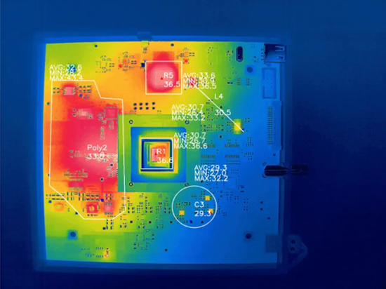
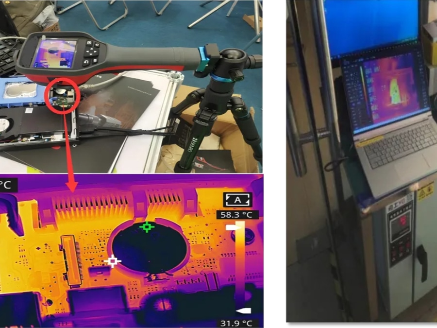
deploying a thermal camera for PCB fault detection and localization
PCB Temperature Measurement
How to Match the Camera to Real Electronics Workflows
The best selection becomes clearer when you map the camera to the workbench, not to a spec sheet.
Board Bring-Up and Prototype Debugging
During first power-on, you need to find unexpected heating fast. A camera with manual focus, good close-range detail, and built-in measurement functions helps you compare regulators, drivers, connectors, and power paths while the board is active.
For this workflow, prioritize:
Close focus or macro support.
640×512 resolution if the board is dense.
Radiometric images for later review.
Region measurement for known high-risk components.
The goal is not only to find the hottest part, but also to understand whether the thermal pattern matches your design expectation.
Repair and Failure Analysis
Repair teams often search for components that heat up abnormally compared with rest of the board. This can be a shorted capacitor, damaged IC, current leakage, or connector fault.
Here, macro and focus control move up the list. A lower-cost camera with weak close focus may work for large modules, but miss the component-level detail that makes repair faster. Use a stable mount when possible. Even a good camera loses value if every image is taken at a different distance and angle.
If your main task is board-level troubleshooting, Raythink’s guide to using a thermal camera for electronics repair covers more repair and rework use cases.
Lab Validation and Research
Lab teams need repeatable data. They may compare board revisions, load conditions, firmware settings, enclosure designs, or heat sink materials.
For lab use, look for:
Low NETD for subtle changes.
Radiometric video for startup and load-step tests.
PC analysis and temperature data export.
Custom report templates.
Enough resolution to measure each region without mixing nearby heat sources.
If you publish internal test reports, keep the measurement setup visible in the report: target distance, emissivity, ambient conditions, load profile, and measurement regions.
Electronics Manufacturing and Product Testing
In electronics manufacturing and product testing, engineers may need to resolve small components and obtain repeatable temperature measurements. A high-resolution thermal camera, combined with an appropriate lens and working distance, can help evaluate temperature distribution across circuit boards, prototype assemblies, and compact electronic modules.
Higher detector resolution alone does not guarantee accurate measurements. Reflective surfaces, incorrect emissivity settings, unwanted reflections, and poor focus can all introduce measurement errors. The practical benefit of higher resolution depends on the lens, field of view, working distance, surface emissivity, calibration, and analysis settings used for the test.
Battery Module Electronics and Power Boards
Battery systems add another layer: heat can come from cells, power electronics, connectors, balancing circuits, or enclosure design. A handheld camera is useful during lab evaluation and troubleshooting. Fixed systems may be better for continuous production monitoring when the same battery-related process needs repeated positioning, alarms, and long-term records.
For battery electronics, prioritize temperature range, region measurement, trend recording, and safe working distance. If you need continuous alarms, consider whether a fixed thermal camera or platform software should be part of the project.
For a deeper look at real PCB testing scenarios, see Raythink’s guide to PCB thermal imaging applications.
Raythink Product Examples for PCB and Electronics Inspection
Use these examples as a selection map, not as a universal ranking. The right choice depends on your smallest target, working distance, report needs, and budget.
Product Example Best Fit Key Features
RM620 Circuit design and general electronics diagnostics 640×512, <35 mK, 0.63 mrad IFOV, manual focus,
PC/mobile software
RT400 Expert analysis and mixed lab/field work 480×360, 960×720 super resolution, <35 mK, trend
analysis, PDF reports
RS600 Small components and high-detail diagnostics 640×512, 1280×1024 super resolution, <25 mK,
macro lens support
RS1280 Research and commercial microelectronics detail 1280×1024, 2560×2048 super resolution, <25 mK,
0.34 mrad standard IFOV
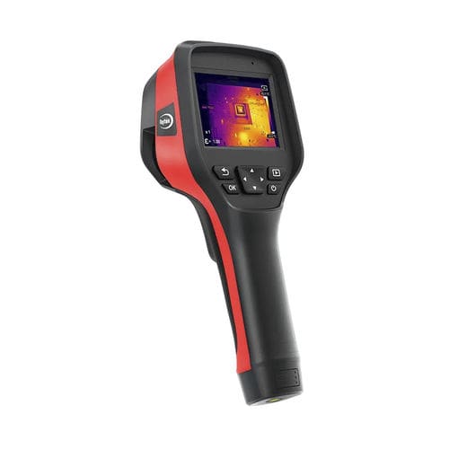
The RM620 handheld thermal camera is a practical starting point when the task is electronic circuit design, general electronics diagnostics, and power board inspection. Its 640×512 detector, <35 mK sensitivity, 0.63 mrad IFOV, and PC/mobile software support make it stronger than a basic screening camera for dense boards.
Choose RM620 when you need a professional handheld camera for circuit design checks and board-level heat comparison. Skip it if your main task is tiny SMD fault isolation that requires confirmed macro lens support.
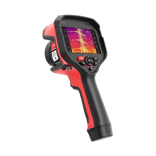
The RT400 Expert Thermal Camera fits teams that need more built-in analysis, trend analysis, and report output. It has 480×360 resolution with 960×720 super resolution, <35 mK NETD, optional wide-angle/telephoto/super-telephoto lenses, up to 15 movable points/lines/areas, trend analysis, radiometric video, PDF report output, and PC editing/template support.
Choose RT400 when the camera will move between lab diagnostics, electrical R&D, routine checks, and report-heavy workflows.
RM620 Handheld Thermal Camera, Handheld Thermal Imager
RM620 handheld thermal camera
RT400 Expert Thermal Camera, Professional Thermal Camera
RT400 Expert Thermal Camera
The RS600 Flagship Thermal Camera is the Raythink handheld option to check when macro capability is required for small-target PCB work. It has 640×512 resolution, 1280×1024 super resolution, <25 mK NETD, optional lens choices, up to 25 movable measurement objects, trend analysis, radiometric video, PDF reports, and PC/mobile software.
Choose RS600 when you need macro capability, strong sensitivity, and enough detail for small components, high-end lab work, or electronics failure analysis.
The RS1280 Flagship Thermal Camera is the high-pixel option for research and microelectronics tasks. Its official page lists 1280×1024 resolution, 2560×2048 super resolution, <25 mK NETD, 0.34 mrad IFOV with the standard lens, and minimum imaging distance down to 0.2 m with the wide-angle lens. It also supports up to 35 points/lines/areas, trend analysis, radiometric video, PDF reports, and PC/mobile software.
Choose RS1280 when the work calls for the most spatial detail, research-grade image density, or repeated analysis across small electronic assemblies. If your main need is very close component inspection, verify the lens and fixture setup against your target size before purchase.
RS600 Flagship Thermal Camera, Professional Thermal Camera
RS600 Flagship Thermal Camera
RS1280 Flagship Thermal Camera, Professional Thermal Imaging Camera
RS1280 Flagship Thermal Camera
Pre-Purchase Checklist
Use this checklist before you choose a PCB thermal imaging camera. It keeps the decision grounded in your real test setup.
I know the smallest component or hot zone I need to measure.
I know the camera-to-board working distance on the bench.
I checked whether the target covers enough pixels for measurement, not only detection.
I confirmed close focus or macro lens support when inspecting small SMD parts.
I checked NETD for low-contrast heating, not only resolution.
I confirmed the temperature range covers my board, module, or power electronics tests.
I can set the emissivity and record the setting in my report.
I have a plan for shiny copper, solder, shielding, and reflective packages.
I can save radiometric images or video for later review.
I can draw measurement areas around components or board zones.
I can export data or create reports if lab documentation is required.
I checked tripod or fixture options for repeatable image capture.
I know whether the project needs handheld inspection, fixed monitoring, or both.
Two items deserve extra attention: macro capability and data workflow. Many cameras can show a hot board. Fewer cameras can separate tiny components at a fixed bench distance and then produce data your team can review weeks later.
Conclusion
The right thermal camera for PCB inspection starts with your target size, working distance, and documentation needs. Resolution helps, but it is only one part of the choice. Close focus, macro lens support, NETD, emissivity control, radiometric files, region measurement, and PC reporting all affect whether the camera gives you useful engineering data.
For repair and board bring-up, focus on close-range clarity and macro capability. For lab validation, add radiometric video, trend curves, and repeatable reports. For research and commercial microelectronics testing, high-pixel models can give the extra spatial detail your work demands.
If you are comparing Raythink handheld thermal cameras for PCB, electronics R&D, or small-target measurement, contact Raythink with your target size, working distance, and reporting requirements.
FAQ
Do I need a macro lens for PCB inspection?
You need a macro lens when your target is a small component, solder joint, trace, or dense board area that a standard lens cannot separate clearly. Macro support helps the camera focus closer and capture more useful detail at a close distance. If you inspect larger power modules, connectors, enclosures, or battery pack surfaces, a standard lens with good manual focus may be enough.
Is 640×512 resolution enough for electronics R&D?
640×512 is enough for many electronics R&D tasks, especially board bring-up, power board inspection, connector heating, and component comparison. It becomes limiting when the target is very small, the board is dense, or the test requires fine spatial detail across many components. In those cases, a 1280×1024 camera may reduce guesswork and improve repeatability.
How do I measure shiny solder, copper, or metal shields?
Measure shiny surfaces carefully because they can reflect infrared energy from the room, your hand, lights, or nearby hot parts. Set emissivity for the material, avoid steep viewing angles, and compare similar surfaces when possible. For lab validation, many teams use matte high-emissivity tape or coating on defined test points when the process allows it. Always record the method in the report.
Should I use a handheld or fixed thermal camera for electronics production?
Use a handheld thermal camera for development, failure analysis, sampling, audits, and flexible lab work. Use a fixed thermal camera when the process needs continuous monitoring, repeated positioning, automatic alarms, or integration with production equipment. Many teams use both: handheld cameras for engineering investigation and fixed systems for line monitoring after the thermal risk is understood.