#Industry News
What Is PCB Potting Services
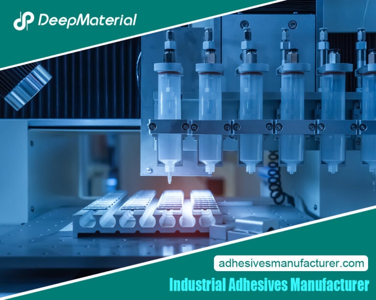
Best PCB Potting Adhesive Glue Manufacturer
PCB potting services involve the process of encapsulating or coating printed circuit boards (PCBs) with a protective material known as potting compound or resin. The primary purpose of PCB potting is to safeguard electronic components and circuitry from environmental factors such as moisture, dust, chemicals, and physical damage. Potting helps enhance the reliability and longevity of electronic devices and systems.
Picking the perfect potting material isn’t easy – it needs to coat your application and cure into a solid protective layer, lasting through whatever environment you throw at it! More often than not, manufacturers go for epoxy resins, polyurethanes, or silicone-based compounds.
Each of these options has their own unique benefits – temperature durability, elasticity against chemicals. But choosing between them is where the real challenge lies.
Potting processes involve five major steps which include preparation, masking, mixing & application, curing and finishing. We will examine the different terms below;
PCB Potting Steps
Preparation – After a good scrub, the PCB is ready to go – shining and spotless, guaranteed free from any type of contaminants.
Masking – Masking off certain parts of the PCB that need to be left uncontained is critical and can help save time in the long run. There are various materials, such as wax or tape, which serve as a safeguard and make sure protected areas don’t get potted.
Mixing & Application – After thoroughly mixing the potting material, per the manufacturer’s instructions of course, it’s time to slather on that gooey goodness all over those components. Whether you pour it in a stream, inject precisely where you need it to be or dispense it with care.
Curing – The potting compound hardens over time, although the duration could differ based on its material make-up. Taking some patience, it eventually solidifies into a durable form – sort of like watching paint dry.
Finishing – With the potting material all set, it’s time to take away those barriers and give our PC board a quality inspection once-over. Not an ounce of cutting corners here – we don’t settle for anything less than perfect!
The Advantages of PCB Potting
PCB Potting, or encasing the electronics in a resilient layer of protection, provides a plethora of advantages towards reliable, strong-built electronic devices and systems. Atop this list hold these key benefits:
Environmental Protection – Potting materials create a barrier that protects electronic components from moisture, preventing corrosion and electrical short circuits. Potting helps seal components against dust, dirt, and other contaminants, reducing the risk of performance degradation.
Chemical Resistance – Potting compounds offer incredible protection against a plethora of chemicals – upping the durability and dependability of electronics in tricky chemical situations. This way, we can ensure our devices stay safe for longer!
Mechanical Properties – Potting the PCB adds that extra touch of durability – think improved impact and shock resistance. More often than not, such reinforcement is critical when you’ve got a device whose environment demands constant handlings or movement.
Heat Management – With its superior thermal conductivity, certain potting materials can rapidly dispel the heat produced by electronic parts. This is key for keeping performance at its peak—not to mention staving off that dreaded overheating!
Improved Electrical Insulation – Avoiding electrical leakage is vital, even more so in operations that involve high-voltage. To reduce the risk of any short circuits from happening, potting materials provide essential insulation. Basically, it’s like a protection layer for safety precautions!
Enhanced Structural Integrity – Potting serves to protect even the most delicate parts from any strain, effectively ensuring that your entire assemblage remains intact. It’s like an armor of safety, keeping everything in place and warding off harshness. Without it, the setup might unravel – far worse than a house of cards!
Corrosion Prevention – Potting is your little savior against environmental corrosion that can otherwise eat away at your electronic components and leave you open to a slew of malfunctioning issues. It’s basically like applying a protective layer, adding extra shelf life on these gadgets and keeping them from corruption-induced breakdowns – something nobody wants!
Customization – Choosing your potting material can be tricky; it all depends on what kind of environment your application needs to thrive in. Temperature-resistance? Flexibility? It’s all got to come into play if you want to get the most out of this stuff. When making a decision like this, make sure that every environmental variable is taken into account before setting things in concrete.
Protecting Sensitive Electronics – Potting creates a shield, making it harder for the wrong kind of people to mess around and take apart devices without proper authorization. It’s like a wall that keeps out any suspicious characters who might get their hands on your electronics. No one can get in with potting – a much-needed layer of protection!
Longer Lifespan – Potting is key to ensuring your electronic devices endure environmental and mechanical stressors, prolonging their life while keeping them in top-notch condition. In other words, this special protecting process plays a major role in the longevity of these gadgets!
PCB potting is a go-to for a variety of industries far and wide. These include auto, aerospace, industrial and consumer electronic sectors where the exposure to tough conditions requires special components. The advantages vary depending on which material is used as well as the unique needs of each application.
Final Thoughts
PCB potting services play a pivotal role in fortifying electronic devices against environmental challenges, ensuring their longevity and reliability. By encapsulating printed circuit boards with protective materials, these services shield components from moisture, dust, chemicals, and mechanical stress.
The resulting benefits encompass enhanced thermal management, improved structural integrity, and resistance to impact and vibration. With customizable potting materials catering to diverse applications, this process secures electronics in fields like automotive, industrial, and aerospace. PCB potting not only safeguards against potential failures but also contributes to the sustained performance and durability of electronic systems in demanding real-world conditions.
For more about a complete guide to the PCB Potting Services, you can pay a visit to Deepmaterial at https://www.adhesivesmanufacturer.com/ for more info.


