#Industry News
PCB Potting Services: A Comprehensive Guide
Best PCB Potting Adhesive Glue Manufacturer
Printed Circuit Boards (PCBs) form the backbone of modern electronic devices, playing a critical role in everything from consumer electronics to industrial machinery. As technology advances, the demand for reliable and durable PCBs has grown exponentially. One key method to enhance the durability and reliability of PCBs is through potting services. This article delves into the world of PCB potting services, exploring what they are, their benefits, the materials used, the processes involved, and their applications in various industries.
What is PCB Potting?
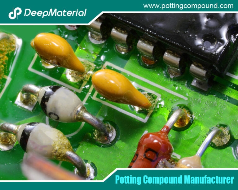
PCB potting involves encapsulating a PCB in a protective material to shield it from environmental factors such as moisture, dust, chemicals, and physical shock. This process not only enhances the PCB’s durability and longevity but also improves its electrical insulation and thermal management properties. Potting is essential for ensuring the reliability and performance of PCBs, especially in harsh or demanding environments.
Benefits of PCB Potting
Environmental Protection: Potting provides a robust barrier against moisture, dust, and other contaminants that can degrade the performance of a PCB.
Mechanical Protection: The encapsulation material absorbs and distributes mechanical stress, protecting the PCB from shocks, vibrations, and impacts.
Electrical Insulation: Potting materials enhance the electrical insulation of PCBs, preventing short circuits and electrical interference.
Thermal Management: Certain potting materials possess excellent thermal conductivity, helping to dissipate heat generated by electronic components.
Chemical Resistance: Potting compounds can protect PCBs from corrosive chemicals and solvents, extending their operational life.
Enhanced Security: Potting can deter tampering and reverse engineering, as it makes accessing the underlying circuitry more difficult.
Materials Used in PCB Potting
The choice of potting material depends on the specific requirements of the application. Common materials include:
Epoxy Resins: Known for their excellent adhesion, mechanical strength, and chemical resistance, they are widely used in PCB potting. They offer robust protection against moisture and thermal stress.
Polyurethane Resins: These resins provide flexibility and excellent moisture resistance. They are ideal for applications where the PCB may be subjected to mechanical stress or vibration.
Silicone Resins: Silicone potting compounds offer superior thermal stability and flexibility. They are suitable for high-temperature applications and provide excellent electrical insulation.
Acrylic Resins: Acrylics are easy to apply and provide reasonable protection against moisture and chemicals. They are often used in applications where reworkability is a priority, as they can be more easily removed than other potting materials.
The Potting Process
The potting process involves several critical steps to ensure that the PCB is adequately protected:
Preparation: The PCB and the potting material must be prepared before the potting process. This involves cleaning the PCB to remove contaminants that could affect adhesion and ensuring the potting material is mixed correctly if it’s a multi-part compound.
Application: The potting material is applied to the PCB, typically through dispensing equipment that allows for precise control over the amount and placement of the material. This step must be carefully controlled to avoid air bubbles and ensure even coverage.
Curing: Once the potting material is applied, it must cure to form a solid, protective layer. Curing times and conditions vary depending on the material used. Epoxy resins, for example, may require heat to cure, while some silicones can cure at room temperature.
Inspection: After curing, the potted PCB is inspected to ensure that the potting process was successful and that there are no defects, such as voids or incomplete coverage. Quality control is essential to ensure the reliability of the potting process.
Applications of PCB Potting Services
PCB potting services are utilized in a wide range of industries and applications, each with specific requirements for protection and performance:
Automotive Industry: In automotive electronics, PCBs are exposed to harsh conditions, including temperature extremes, vibrations, and chemical exposure. Potting ensures the reliability of engine control units, sensors, and infotainment systems.
Aerospace and Defense: PCBs in aerospace and defense applications must withstand extreme conditions and require high reliability. Potting provides the necessary protection for avionics, communication systems, and radar equipment.
Medical Devices: Medical electronics demand high reliability and protection against environmental factors. Potting protects sensitive PCBs in pacemakers, diagnostic equipment, and imaging systems.
Industrial Applications: In industrial environments, PCBs are often exposed to dust, moisture, and mechanical stress. Potting protects control systems, sensors, and other critical electronics.
Consumer Electronics: While less demanding than industrial or automotive applications, consumer electronics also benefit from potting. It provides added durability and protection for smartphones, wearable tech, and home appliances.
Renewable Energy: PCBs in renewable energy systems, such as solar panels and wind turbines, are exposed to outdoor conditions and require protection from moisture and temperature fluctuations. Potting ensures long-term reliability and performance.
Challenges and Considerations in PCB Potting
While PCB potting offers numerous benefits, it also presents specific challenges and considerations:
Material Selection: Choosing a suitable potting material is critical and depends on the application’s specific environmental conditions and performance requirements. Factors such as thermal conductivity, flexibility, and chemical resistance must be considered.
Process Control: The potting process must be precisely controlled to ensure even coverage and avoid defects. This requires specialized equipment and expertise.
Cost: Potting can add to the overall cost of PCB manufacturing. It is essential to balance the benefits of potting with the additional costs to determine if it is the right solution for a particular application.
Repairability: Once a PCB is potted, it can be challenging to repair or rework. This must be considered during the design phase, especially for applications that require future maintenance.
Compatibility: The potting material must be compatible with the PCB components and materials to avoid adverse reactions that could compromise the integrity of the potting.
Future Trends in PCB Potting Services
As technology continues to evolve, so too does the field of PCB potting services. Emerging trends include:
Advanced Materials: Development of new potting materials with enhanced properties, such as higher thermal conductivity, improved flexibility, and better environmental resistance.
Miniaturization: As electronic devices become smaller, potting must adapt to provide protection without adding significant bulk. This requires precise application techniques and advanced materials.
Automation: Increasing automation in the potting process to improve precision, consistency, and efficiency. Automated systems can handle complex potting tasks and reduce the risk of human error.
Sustainability: Growing focus on environmentally friendly potting materials and processes. This includes the development of biodegradable and recyclable potting compounds.
Integration with Other Technologies: Combining potting with other protective technologies, such as conformal coating and encapsulation, to provide multi-layered protection for PCBs.
Conclusion
PCB potting services play a crucial role in enhancing printed circuit boards’ durability, reliability, and performance across a wide range of industries. By providing robust protection against environmental factors, mechanical stress, and electrical interference, potting ensures that PCBs can withstand the demands of their operating environments.
As technology advances, the importance of potting in PCB manufacturing is likely to grow, driven by the need for more durable and reliable electronic devices. By understanding the benefits, materials, processes, and challenges associated with PCB potting, manufacturers can make informed decisions to optimize the protection and performance of their products.
For more about choosing the Top PCB Potting Services: A Comprehensive Guide, you can pay a visit to DeepMaterial at https://www.pottingcompound.com/ for more info.


