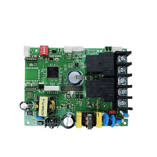
#Product Trends
Application of Multilayer PCB Design in PCBA
Application of Multilayer PCB Design in PCBA
A multilayer PCB (Printed Circuit Board) is a printed circuit board made up of three or more conductive layers, typically separated by dielectric layers to ensure insulation between each layer. With the increasing demands for compactness, performance, and signal integrity, multilayer PCBs have become a widely applied option in PCBA (Printed Circuit Board Assembly) due to their unique design structure and superior performance. This article will explore the applications of multilayer PCB design in PCBA and its importance in the manufacturing process.
I. Characteristics of Multilayer PCBs
1. High-Density Routing: Multilayer PCB design supports denser wiring, allowing more functions to be achieved in limited space.
2. Stable Signal: The multilayer structure helps reduce electromagnetic interference, improving the stability of signal transmission.
3. Power Management: Dedicated power layers in multilayer PCBs effectively distribute current and reduce power noise.
II. Advantages of Multilayer PCB in PCBA
1. High Space Utilization Efficiency: In compact electronic products, such as smartphones and wearable devices, internal space is extremely limited. The structure of multilayer PCBs enables more circuitry to be integrated within limited space, enhancing assembly density and enabling complex functionalities.
2. Signal Transmission Quality: Multilayer PCBs effectively reduce signal interference, which is crucial for high-speed electronic devices where signal speed and quality are vital. Electromagnetic interference shielding helps ensure signal integrity and stability.
3. Enhanced Current Carrying Capacity: The structure of multilayer PCBs facilitates better management of power and ground lines, thus reducing power noise and ripple. In high-power devices, this capability is essential to prevent power fluctuations from affecting the equipment.
4. Higher Design Flexibility: Multilayer PCBs offer greater design flexibility, allowing designers to freely arrange circuit layouts, optimize signal paths, and improve routing efficiency. This flexibility makes multilayer PCBs perform exceptionally well in complex electronic devices.
III. Considerations in Multilayer PCB Design
1. Number of Layers: The complexity of the device, signal requirements, and product cost often determine the number of PCB layers. TECOO flexibly determines the number of layers based on customer needs and industry standards, ensuring optimal performance and cost-effectiveness.
2. Signal Integrity and Power Distribution: The distribution of signal and power layers in multilayer PCBs must be reasonable to ensure high-quality signal transmission.
3. Thermal Management: Multilayer PCBs, due to their compact structure, are prone to heat buildup, so thermal management is essential in the design phase.
IV. Impact of Multilayer PCB Design on PCBA Manufacturing
1. High Precision Requirements for Layer Alignment: Multilayer PCBs generally consist of three or more conductive layers, and these layers require precise alignment to ensure proper connections of all electrical signals and power paths; otherwise, it may lead to short circuits or unstable signals.
2. Requirements for Drilling Processes: Drilling is a key step in multilayer PCB manufacturing. High precision is especially needed for via and blind via designs to ensure effective interconnections between layers.
3. High Demands on SMT and Soldering Processes: The complexity of multilayer PCBs adds to the challenges of PCBA manufacturing, requiring higher precision in surface mount and soldering processes. With different layout levels, some solder points may be at varying heights or hidden in middle or bottom layers, making the precision of SMT machines and soldering equipment particularly important.
4. Cost Control Challenges: Due to their complexity, multilayer PCBs typically lead to higher manufacturing costs. The additional conductive layers and higher precision requirements in processes make production more intricate, increasing both equipment and labor costs.
TECOO has accumulated extensive experience in the design and manufacturing of multilayer PCBs, ensuring efficient interconnection between each circuit layer through optimized design to meet customer demands for product miniaturization and high performance. Whether in consumer electronics, industrial equipment, or medical devices, TECOO provides high-quality solutions in multilayer PCBA design to meet diverse customer needs.


