#Industry News
PCB Cloning & Prototyping: A Complete Guide for Faster, Smarter Electronic Development
From Reverse Engineering to Rapid Prototyping—Everything You Need to Know
In modern electronic product development, PCB cloning (circuit board copying) and prototyping have become essential tools. Whether it’s for upgrading legacy products, repairing discontinued equipment, or conducting competitive benchmarking, PCB cloning enables companies to quickly reproduce circuit designs. Prototyping then validates these designs before they move into mass production.
This guide walks you through the PCB cloning process, key technologies, and common FAQs—helping you complete projects with speed, accuracy, and confidence.
1. What is PCB Cloning?
PCB cloning, also known as circuit board reverse engineering, is the process of recreating the original PCB design files (such as Gerber files, schematics, and BOM lists) by means of disassembly, scanning, and mapping.
Typical Applications of PCB Cloning:
Product Repair & Replacement – Reproducing discontinued PCBs for legacy systems
Competitive Analysis – Studying rival product designs for insights
Redesign & Optimization – Enhancing performance or lowering production costs
IP Verification – Checking whether your designs have been illegally copied
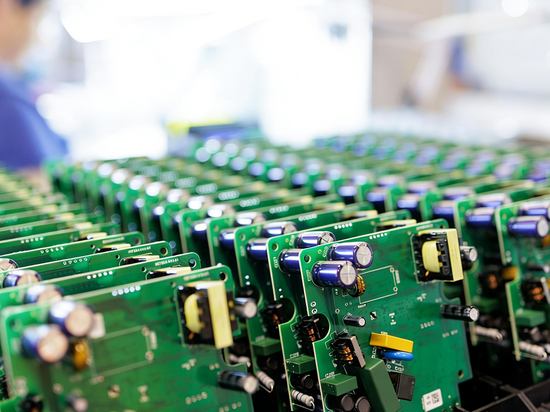
2. Standard PCB Cloning Workflow
Step 1: Disassembly & Scanning
Precision optical or X-ray scanning to capture PCB layer structures
Documentation of all components, layouts, and trace patterns
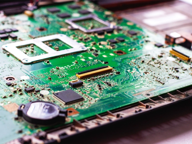
Step 2: Image Processing & Layer Reconstruction
Using EDA tools (Altium, Cadence, etc.) to rebuild copper traces
Identifying top, bottom, and internal layers to restore circuit connections
Step 3: Schematic & BOM Creation
Reverse-engineering circuit schematics from the reconstructed board
Generating a detailed BOM with part numbers, specifications, and sourcing options
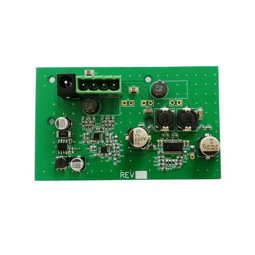
Step 4: Gerber Output & Prototyping
Producing Gerber files for PCB manufacturing
Running small-batch prototypes to confirm performance
3. Key Technologies in PCB Cloning
Multilayer PCB Cloning
Traditional method: layer sanding + scanning (risk of damage)
Advanced method: X-ray CT scanning for non-destructive data acquisition
High-Frequency & High-Speed PCB Cloning
Special focus on impedance matching and signal integrity
Validation with Vector Network Analyzer (VNA)
Chip Decryption & Firmware Extraction
Required for some MCUs (e.g., STM32)
Must comply with IP laws to avoid infringement risks
4. FAQs About PCB Cloning & Prototyping
Q1: Is PCB cloning legal?
Legal: For repairs, research, or authorized redesigns
Risk: Unauthorized commercial duplication may violate IP rights
Q2: How accurate is the cloning process?
Standard PCBs: ±0.05 mm tolerance
HDI boards: Require laser scanning + 3D modeling for precision
Q3: How to ensure prototype success?
Partner with professional EMS providers like TECOO
Perform DFM analysis, AOI testing, and flying probe verification
Q4: What’s the timeframe & cost?
2–4 days for simple boards, 1–2 weeks for complex multilayers
Cost depends on complexity but usually lower than new design development
5. Choosing the Right PCB Cloning Service Provider
A trustworthy partner should provide:
a. Proven Experience – Handling multilayer & high-frequency boards
b. Advanced Equipment – High-resolution scanners, X-ray systems, etc.
c. Legal Compliance – Reverse engineering with strict IP safeguards
d. Full Service – From cloning → optimization → prototyping → production
6. Why Partner with TECOO?
a. 20+ Years of Expertise – Serving automotive, medical, and industrial sectors
b. Military-Grade Precision – Reverse engineering for 1–32 layer and high-frequency PCBs
c. Rapid Prototyping – Delivery in 3–5 days with free DFM analysis
d. Secure & Compliant – Strict NDAs and data protection standards
Contact TECOO today for professional, reliable PCB cloning & prototyping services.