#Industry News
How DFM (Design for Manufacturing) Elevates Your PCB Project
A Practical Guide to Ensuring Your PCB Design Translates into High-Yield, Cost-Effective, and Reliable Manufacturing
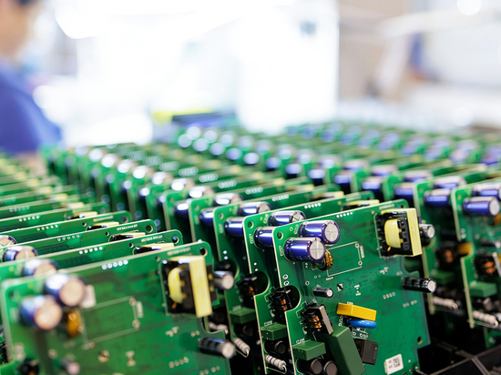
In the fast-moving electronics landscape, even the best circuit design is only the starting point. Many engineering teams still encounter the same problem: a schematic or simulation that looks flawless turns into a challenge during actual PCB fabrication and assembly. Unexpected defects, unnecessary costs, schedule overruns, and multiple rounds of rework often appear once the design hits the production floor.
In most cases, these setbacks stem from insufficient attention to DFM—Design for Manufacturability.
Having supported global hardware companies for more than two decades, TECOO knows that DFM is far more than a final design review. It is an engineering mindset that begins at the earliest stage of development, ensuring that every PCB is optimized for real-world manufacturing processes, long-term reliability, and scalable production.
I. What Is DFM? A Strategic Approach, Not a Simple Checklist
DFM (Design for Manufacturability) is an engineering discipline that incorporates manufacturing constraints—such as PCB fabrication limits, assembly requirements, material specifications, and supply chain realities—directly into the design process.
In other words, DFM ensures your design is not just functional on paper but fully compatible with mass production, automated assembly, and stable, repeatable manufacturing outcomes.
It bridges the gap between electronic design theory and the physical environment where the product is actually built.
II. The Consequences of Overlooking DFM: Risks That Can Derail Your Project
Failing to conduct DFM analysis exposes your project to significant and costly issues. Some of the most common include:
1. Increased Fabrication and Assembly Costs
Design choices that do not align with standard PCB capabilities—such as irregular pad shapes, unusual spacing, or non-standard stack-up requirements—often lead to higher fabrication prices. Poor component layout also slows down SMT assembly and increases machine setup or manual labor time.
2. Lower Yields and Frequent Rework
Small oversights in pad geometry or land pattern design can create soldering defects such as bridging, tombstoning, cold joints, or insufficient wetting. Imbalanced thermal design may cause warping or component stress during reflow.
3. Compromised Product Reliability
Weak EMC strategies, poor grounding, or flawed power distribution networks can cause intermittent failures that only show up under real operating conditions—long after the prototype appears to work fine.
4. Delays That Push Your Product Behind Schedule
Manufacturing issues discovered late typically force redesign, re-prototyping, and additional validation, significantly delaying time-to-market and increasing total development cost.
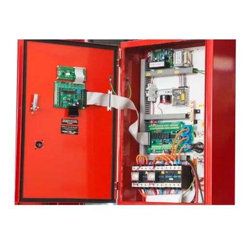
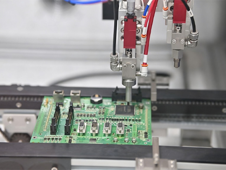
III. How TECOO’s DFM Services Reinforce the Success of Your PCB Project
Every PCB and PCBA project handled by TECOO undergoes an extensive DFM evaluation. When your design files are submitted, our engineers apply advanced analysis tools and deep manufacturing knowledge to assess the manufacturability of your design from multiple angles.
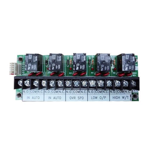
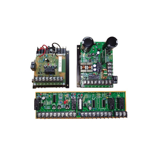
1. PCB Fabrication Review
Verify minimum trace width, spacing, and pad geometry
Check hole-to-copper clearances and via structures
Review stack-up and layer configurations for impedance and signal stability
2. Component Placement and Footprint Validation
Confirm that spacing prevents soldering interference and shadowing
Ensure footprint dimensions match actual, available components
Evaluate thermal design around heat-generating parts
3. Assembly Feasibility (SMT/THT)
Validate compatibility with automated pick-and-place equipment
Examine pad design for robust solder joints
Ensure adequate provision for test points, inspection, and manual rework
4. Design for Testability (DFT)
Review test point accessibility and coverage
Confirm that the finished board can be fully tested before shipment
Strengthen long-term reliability by enabling thorough production testing
After analysis, TECOO provides a clear, actionable DFM report highlighting potential issues and recommending improvements. Our engineering team can collaborate directly with your designers to implement solutions before fabrication begins.
IV. Why Choosing TECOO for DFM Brings Exceptional Value
Incorporating DFM early—and working with a manufacturing partner who understands it deeply—translates into measurable advantages:
1. Significant Cost Reductions
By designing to standard processes and materials, yields increase and waste decreases, lowering overall production expenses.
2. Faster Time-to-Market
Avoid design iterations caused by manufacturability problems. Move from design to production smoothly and efficiently.
3. Higher Reliability and Long-Term Performance
Identifying risks early prevents field failures, extends product lifetime, and enhances user satisfaction.
4. A More Stable Supply Chain
With strong sourcing experience, TECOO can recommend components with healthy availability and cost efficiency, reducing procurement risks.
Conclusion
Success in modern electronics depends not only on innovative design but also on the ability to manufacture consistently at scale. DFM is one of the most valuable investments you can make for the entire lifecycle of your product.
By partnering with TECOO, you gain a team committed to guiding your project from initial concept through mass production. With over 20 years of EMS expertise, we provide the insights and processes necessary to avoid costly errors and ensure your product is both manufacturable and dependable.
Contact TECOO today to receive a complimentary DFM analysis for your next PCB design.
Together, we can build a product that is reliable, manufacturable, and ready for the market.