
#Industry News
Why AlN Ceramic Is Becoming Important for High-Power CW DFB Laser Packaging
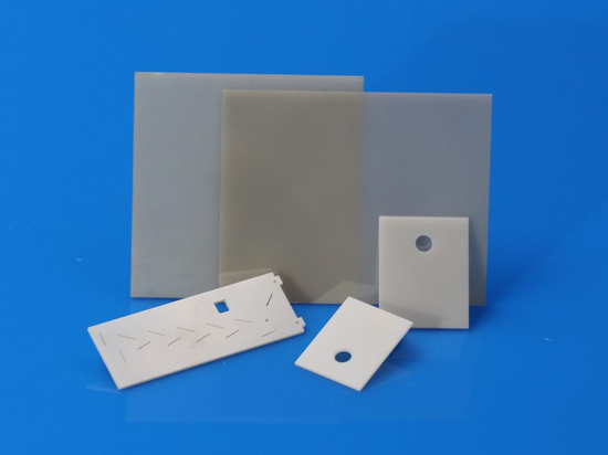
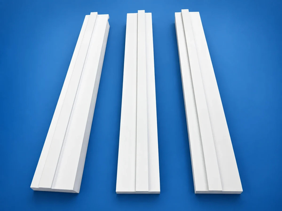
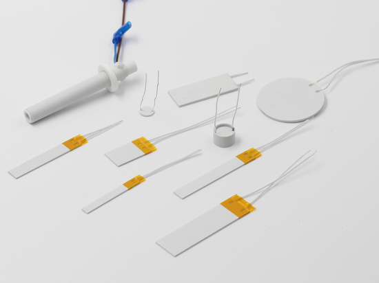
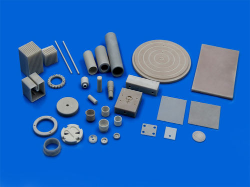
AlN Ceramic Submount
From laser junction temperature and package thermal resistance to submount material selection
As CW DFB lasers move toward higher output power for external laser sources, silicon photonics and next-generation optical interconnects, the packaging challenge is changing. The question is no longer only whether a laser can reach the required optical power, but whether that power can be maintained at elevated operating temperatures without excessive junction-temperature rise.
This puts the thermal path beneath the laser die under much greater scrutiny. As heat flux increases, the submount becomes an increasingly important part of package thermal resistance – and this is where aluminum nitride (AlN) ceramic can provide a useful combination of thermal, electrical and mechanical properties.
1. High Optical Power Is Not Enough – Power at Temperature Matters
High-power CW DFB lasers are expected to provide stable continuous optical output while meeting demanding requirements for wavelength stability, efficiency, noise and reliability. A room-temperature peak-power value therefore tells only part of the story.
As electrical input and optical output increase, more heat must be removed from a very small active region. If the package cannot conduct that heat efficiently, laser junction temperature rises. The practical engineering target becomes a combination of optical power, operating temperature and lifetime rather than optical power alone.
Higher Optical Power → Higher Heat Flux → Higher Junction Temperature Risk → Lower Package Thermal Resistance Required
2. Why Junction Temperature Matters
Ambient temperature is important, but the laser die responds more directly to its junction temperature. A rise in junction temperature can influence threshold current, slope efficiency, emission wavelength and long-term degradation behavior.
For continuous-wave operation, heat is generated continuously. The thermal design objective is therefore to minimize the temperature rise between the active junction and the cooling structure while maintaining optical, electrical and mechanical stability.
For package engineers, this shifts attention from the external heat sink alone to every layer beneath the die.
3. The Thermal Path Inside a CW DFB Laser Package
A simplified heat-flow path can be represented as:
Laser Junction → Laser Die → Die Attach → Submount → TEC / Package Base → Heat Sink
Each layer and interface contributes thermal resistance. The total junction-to-package thermal performance is therefore determined by the complete stack, not by one material property.
As laser heat flux increases, the submount becomes important because it sits directly beneath the heat source and must transfer and spread heat toward the next cooling layer.
aluminum nitride ceramic heat sink
4. Why the Submount Becomes Critical at Higher Heat Flux
A laser submount is more than a mechanical support. It can simultaneously provide a die-attach surface, heat-spreading path, electrical isolation and metallized interconnection.
At moderate heat loads, conventional ceramic substrates such as alumina may provide sufficient performance. At higher heat flux, however, thermal resistance through the submount can become a more significant part of the total package thermal path.
This is the point at which a higher-thermal-conductivity electrically insulating ceramic becomes valuable.
aluminum nitride ceramic heat sink
5. Why AlN Works as a Laser Submount Material
The value of AlN is not thermal conductivity alone. Its usefulness in laser packaging comes from a combination of properties that are difficult to obtain from a single material.
High thermal conductivity: helps reduce the temperature drop through the ceramic and supports heat spreading beneath a concentrated laser heat source.
Electrical insulation: allows the ceramic to conduct heat while electrically isolating the device or package structure.
Relatively low thermal expansion: provides useful compatibility with semiconductor packaging and can help control thermomechanical stress in a properly designed assembly.
Precision surface capability: controlled thickness, flatness, parallelism and surface finish support die attachment and optical assembly.
Metallization compatibility: patterned metallization can provide die-attach areas, electrical routing and bonding surfaces.
For this reason, AlN can function not simply as a ceramic plate, but as a thermally functional packaging element.
Laser Ceramic Submount
6. AlN Alone Does Not Guarantee Low Thermal Resistance
Using a high-conductivity AlN ceramic does not automatically guarantee a low laser junction temperature. A high-conductivity ceramic cannot compensate for a poor thermal interface.
An excessively thick or voided die-attach layer can dominate interface resistance.
Poor flatness can reduce effective contact area.
Metallization and solder structures add additional layers to the thermal path.
An undersized submount can limit lateral heat spreading.
Poor contact to the TEC or package base can reduce the benefit of the ceramic.
This is why the AlN submount should be evaluated as part of the complete junction-to-cooling thermal stack rather than as an isolated material.