#Product Trends
Aluminum Nitride Substrate Selection Guide: Thermal Conductivity, Thickness, Surface Finish and Qualification
Aluminum Nitride Substrate
Start with the thermal resistance budget
Aluminum nitride substrate selection begins with the allowable temperature rise, device power loss and heat-flow path. Establish how much thermal resistance the ceramic layer can contribute after accounting for die attach, metallization, interfaces and the cooling structure.
For steady, one-dimensional conduction through a uniform layer:
Rth = t / (k × A)
Here, Rth is thermal resistance in K/W, t is thickness in metres, k is thermal conductivity in W/(m·K), and A is the cross-sectional heat-transfer area in m². The temperature difference across this layer is ΔT = Q × Rth, where Q is the heat passing through it in watts.
Use this relationship to compare candidate designs. A small heat source on a larger substrate introduces lateral heat spreading, so neither the full substrate area nor the device footprint should automatically be treated as a uniform conduction area. Final temperature predictions require an appropriate thermal model or measurements on the assembled device.
Select thickness together with insulation and manufacturability
At constant conductivity and area, ceramic-layer resistance is proportional to thickness. Reducing thickness from 0.635 to 0.38 mm reduces this resistance by approximately 40%. This can be a useful alternative to changing conductivity grade, provided the thinner part meets electrical and mechanical requirements.
A thinner substrate also changes handling, clamping, singulation and assembly conditions. Check support span, hole and edge geometry, metallization stresses and damage during transfer. Material dielectric strength alone does not establish a safe operating voltage: electrode geometry, insulation distances, voltage waveform, test duration and the assembled insulation system must also be evaluated.
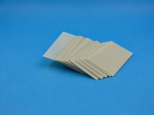
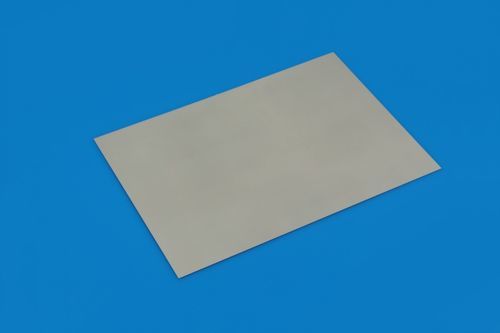
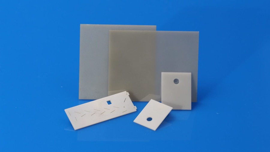
Choose the panel format around the downstream equipment and usable area. A 138 × 190 mm production panel can be a starting point, but the best layout depends on edge exclusions, tooling features and cutting allowances. Compare cost per accepted finished part, including machining, inspection and yield, rather than cost per panel alone.