#Product Trends
Lapped and Polished Aluminum Nitride Substrates
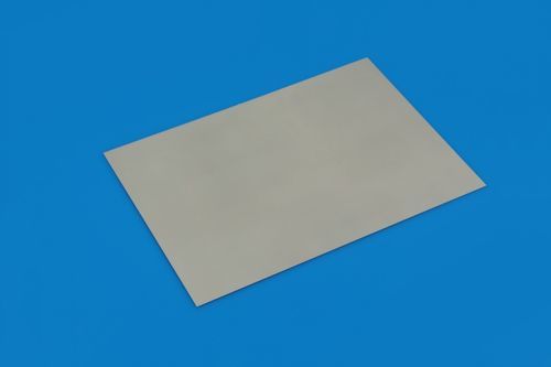
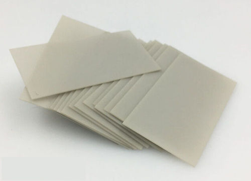
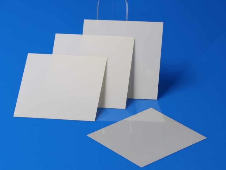
Aluminum Nitride Ceramic Sheet
INNOVACERA supplies ground, lapped and polished aluminum nitride (AlN) substrates for thin-film circuits, laser diode submounts, photonics and precision metallization. Thermal conductivity we provided is 170, 200 and 230 W/m·K, with master sizes up to 138 × 190 mm. For applications requiring a fine surface, precision polishing is available down to Ra ≤ 0.05 μm, with custom sizes, thickness,and slots available.
AlN substrate surface finish can be selected according to the downstream process. INNOVACERA provides grinding, fine lapping, polishing and precision polishing, together with custom thicknesses, dimensions and machining features for different application requirements.
Flatness, Warpage and TTV
Flatness and TTV are specified according to substrate size, thickness and measurement method. For precision applications, requirements can be evaluated against the customer drawing and defined inspection area. Warpage below 0.3% is available on specified production configurations.
Finish Roughness
Grinding is Ra 0.3–0.6 μm. Fine lapping, 0.1–0.4. Polishing gets under 0.10, precision polishing to 0.05 and below. A substrate that only has to move heat is fine at grinding. An LD submount or a thin-film circuit grinding is not enough, because the next step, whether deposition, litho or die attach, cares about more than the surface. AlN substrates for thin-film processing, DPC and precision metallization generally require a lapped or polished surface before subsequent customer processing.
Inspection
Inspection can include dimensions, thickness, roughness, warpage, flatness and edge quality. Density, thermal conductivity and other material properties can be verified according to project requirements. Inspection reports are available for production programs when required.