#Product Trends
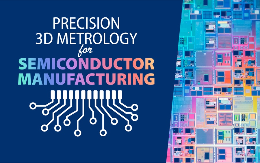
Precision 3D metrology for semiconductor manufacturing
Discover how 3D optical metrology meets the challenges posed by semiconductor manufacturing.
Semiconductors are at the heart of modern life, powering everything from simple devices like thermometers and LED lighting to smart appliances, as well as the advanced systems behind smartphones, computers, and self-driving cars. Everyday actions such as paying with a card, browsing the internet, or following GPS navigation depend on their performance, making chips indispensable to how we live and connect.
Beyond consumer electronics, semiconductors are the foundation of industrial automation, healthcare technology, and cloud computing. They enable robotics in factories, advanced medical imaging, AI applications, and large-scale data processing. Nearly every action we take today is supported by these tiny components, the invisible force that drives the modern world.
Semiconductors: Powering modern technology
Over the past seventy years, the semiconductor industry has grown into the world’s largest manufacturing sector, producing more chips than any other product. Continuous advances in miniaturization and performance, as described by Moore’s Law, have fueled breakthroughs in computing, communications, and automation. Today, rising demand for faster, more efficient, and more innovative technologies is driving growth in artificial intelligence, autonomous vehicles, and the Internet of Things.
With more than 90 percent of electronic devices relying on chips, the market shows no sign of slowing. Global revenues are expected to increase by 15 percent in 2025, with equipment sales projected to exceed 100 billion dollars. At the same time, the number of connected devices is expected to surpass 30 billion IoT units by 2030, further driving demand and creating new opportunities for innovation and long-term industry growth.
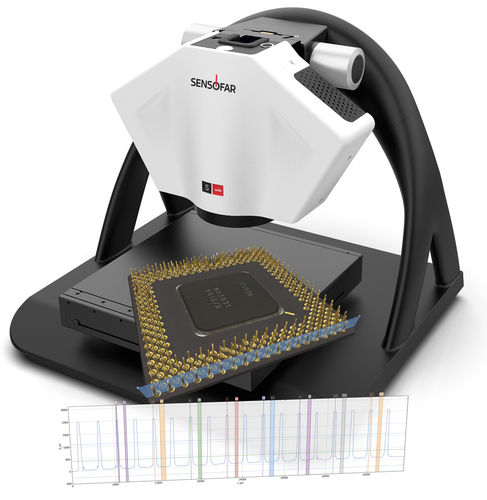
The critical role of 3D optical metrology in modern manufacturing
As semiconductor technology advances, ensuring accuracy, reliability, and efficiency throughout production becomes increasingly complex. With chips requiring hundreds or even thousands of fabrication steps, process control and quality assurance are crucial to maintaining yield, minimizing downtime, and controlling costs.
Metrology plays a vital role in meeting these demands.
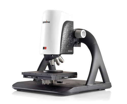
Sensofar’s 3D optical metrology solutions provide non-contact, high-resolution surface analysis, capturing dimensions, roughness, and defects with sub-nanometer precision while preserving delicate structures. From wafer preparation to final inspection, these technologies enable manufacturers to optimize processes and maintain the highest quality standards throughout the semiconductor workflow.