#Product Trends
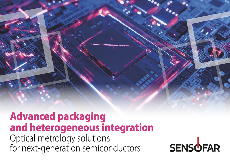
Advanced packaging and heterogeneous integration
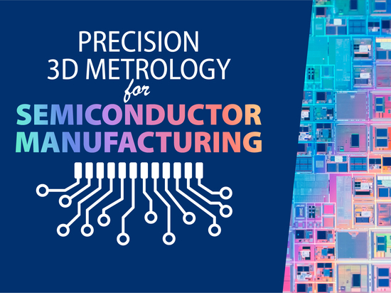
Optical metrology solutions for next-generation semiconductors
The semiconductor industry is advancing at a remarkable pace to meet the growing demand for enhanced performance, improved energy efficiency, and increasingly compact designs. As conventional scaling reaches its physical and economic boundaries, new strategies such as heterogeneous integration and advanced packaging have become critical. These approaches are transforming system design by combining different functionalities in a single package and enhancing interconnectivity, making it possible to deliver powerful, miniaturized solutions for next-generation technologies.
More Moore, More than Moore: Shaping the Future of Semiconductors
Innovation in the semiconductor industry is increasingly shaped by two complementary paradigms: “More Moore” and “More than Moore.”
The “More Moore” pathway continues the pursuit of transistor scaling in line with Moore’s Law, which predicts a doubling of transistors on a chip approximately every two years, boosting both performance and efficiency. Yet as transistors shrink to ever smaller dimensions, this approach faces growing technical and economic hurdles. Even so, optimization remains vital, especially in fields such as high-performance computing and artificial intelligence, where maximizing computational power is essential.
The “More than Moore” paradigm, on the other hand, emphasizes functional diversification rather than scaling. It combines technologies such as sensors, RF modules, photonics, and power electronics into a single package, enabling solutions tailored to specific applications. This is made possible through heterogeneous integration, a process that combines different types of chips with varied functions into a single system. The rise of the Internet of Things, autonomous mobility, and personalized healthcare continues to drive this trend, demanding compact, multifunctional solutions that extend beyond the limits of traditional scaling.
Together, the “More Moore” and “More than Moore” paradigms are driving the ongoing evolution of semiconductor technology, even as the pace of Moore’s Law slows. Both rely heavily on advanced packaging, a set of manufacturing methods that enhance chip assembly and interconnection to deliver higher performance, improved thermal control, and a reduced footprint.
Solutions such as system-in-package (SiP) and 2.5D/3D integration are central to this progress.
Heterogeneous integration and advanced packaging are crucial for the next generation of semiconductors, enabling various materials, technologies, and functions to coexist in compact, efficient systems. These innovations support breakthroughs in high-performance computing, IoT, 5G communications, automotive electronics, and photonics, meeting the need for greater bandwidth, higher energy efficiency, and miniaturization. Each integration approach, from 2.5D and 3D architectures to co-packaged optics and advanced PCBs, presents unique metrology challenges that require precise, high-resolution measurement tools to ensure performance and reliability.
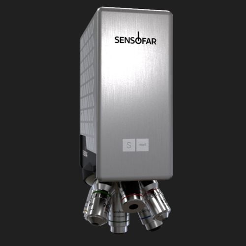
Sensofar’s 3D optical profilometers address these needs with the accuracy, repeatability, and automation required for advanced packaging and heterogeneous integration. Combining industry-leading Interferometry, Confocal, and Focus Variation techniques, they deliver non-contact, high-resolution 3D measurements that are critical for wafer-level inspection, bonding interface analysis, TSV depth profiling, and interconnect characterization. With automated analysis and SDK integration, these systems enhance productivity while enabling manufacturers to maintain process control, improve yields, and accelerate innovation.
As semiconductor technology continues to advance, 3D metrology will remain a cornerstone of process optimization and quality assurance. By providing cutting-edge measurement solutions, Sensofar equips manufacturers with the tools to further enhance semiconductor performance, enabling the creation of faster, smaller, and more energy-efficient devices for the future.